IC Packaging Manufacturing: An Overview of Advanced Packaging Processes
IC packaging manufacturing is the stage of semiconductor production in which a fabricated integrated circuit is assembled into a physical package that protects the chip.
After a semiconductor wafer has gone through chip fabrication, individual dies must be separated, connected, protected, tested, and prepared for integration into products such as computers, vehicles, communication equipment, industrial electronics, and mobile devices.
Traditional semiconductor packages commonly use a substrate, bonding wires, solder connections, or other structures to connect the die with external circuitry. As chips have become more complex, packaging has developed from a protective enclosure into an important part of system design. Modern semiconductor packaging equipment supports processes that can place, connect, mold, inspect, and test semiconductor components with increasingly precise control.
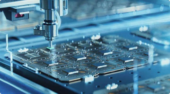
IC packaging equipment can include die attach machines, wire bonders, flip-chip equipment, molding systems, inspection tools, wafer handling equipment, and package testing systems. More advanced semiconductor packaging machinery can also support chiplets, 2.5D integration, 3D stacking, redistribution layers, and hybrid bonding.
From Conventional Packaging to Advanced Integration
Conventional integrated circuit packaging generally connects one semiconductor die to a package substrate. Advanced approaches can combine several dies or chiplets within one package, allowing different types of semiconductor components to work together.
Advanced IC packaging systems may use techniques such as flip-chip assembly, fan-out packaging, wafer-level packaging, 2.5D integration, and 3D stacking. These approaches require close coordination between materials, equipment, process controls, inspection, and testing.
Main Stages of IC Packaging
A typical packaging flow can contain several stages:
- Die preparation separates and prepares individual semiconductor dies.
- Die attach places a die onto a substrate, carrier, or another structure.
- Interconnection creates electrical paths through wire bonding, bumps, redistribution layers, or direct bonding.
- Encapsulation protects the semiconductor structure from physical and environmental effects.
- Inspection checks alignment, connections, surfaces, and package characteristics.
- Testing evaluates electrical and physical behavior before the packaged device enters another stage of production.
The exact sequence varies according to package architecture and semiconductor application.
Importance
IC packaging is important because the package provides the physical and electrical interface between a semiconductor die and the rest of an electronic system. Packaging influences how components are connected, protected, cooled, tested, and integrated into a larger device.
The topic affects consumers indirectly because packaged semiconductors are present in many products used every day. Computers, smartphones, vehicles, telecommunications equipment, appliances, medical electronics, and industrial control systems all depend on semiconductor components.
Supporting Smaller and More Complex Systems
As semiconductor designs become more densely integrated, the connections between chips must also handle increasing amounts of data. Semiconductor assembly equipment therefore needs to support accurate placement and increasingly dense interconnections.
Chip packaging equipment can be used for conventional packages as well as newer structures that combine multiple dies. In a chiplet-based design, several smaller semiconductor dies can be assembled into one package rather than placing every function on a single large die.
Improving Manufacturing Control
Precision IC packaging systems use controlled movement, alignment, temperature, pressure, and material handling. High precision semiconductor packaging machines may incorporate optical inspection and measurement systems to detect alignment errors or other process variations.
Automated semiconductor assembly systems can coordinate several production stages while collecting process information. This can help manufacturing teams identify variations and maintain consistent process conditions.
Packaging and Thermal Management
Packaging also has a role in removing heat from semiconductor devices. Higher processing activity can produce more heat, making thermal paths, package materials, heat spreaders, and cooling structures important design considerations.
Advanced semiconductor packaging equipment must therefore accommodate not only electrical connections but also mechanical and thermal requirements. These considerations become particularly important when several dies or memory components are integrated into the same package.
| Packaging Approach | General Structure | Common Process Characteristics |
|---|---|---|
| Wire bonding | Die connected with fine wires | Die attach, wire bonding, encapsulation |
| Flip-chip | Die connected through bumps | Accurate placement and reflow or bonding |
| Fan-out packaging | Connections redistributed outside die area | RDL formation and molding |
| 2.5D integration | Dies connected through an interposer | Fine interconnects and multiple-die assembly |
| 3D integration | Dies or tiers stacked vertically | Vertical connections and precise bonding |
| Hybrid bonding | Direct connection between prepared surfaces | Very clean surfaces and accurate alignment |
Recent Updates
From 2024 through 2026, advanced semiconductor packaging has increasingly focused on chiplets, hybrid bonding, 2.5D and 3D integration, panel-level packaging, and high-density interconnects. Industry discussions have also connected these technologies with artificial intelligence, high-performance computing, memory integration, and heterogeneous system design.
Growth of Chiplet-Based Packaging
Chiplet architectures divide functions across multiple smaller dies that can be assembled within one package. This approach has encouraged development of new semiconductor packaging machines and assembly processes capable of handling multiple components with precise alignment.
Industry work around the Universal Chiplet Interconnect Express, or UCIe, has also supported discussion of standardized die-to-die communication. Research published through IEEE describes chiplet integration as an important direction for multidie systems and examines different package structures for connecting dies.
Development of Hybrid Bonding
Hybrid bonding has received substantial attention because it can create dense connections between semiconductor structures. The technique joins prepared surfaces containing conductive and insulating regions, making precise surface preparation, alignment, cleanliness, and process control important.
Recent technical work has examined wafer-to-wafer and die-to-wafer hybrid bonding. In 2026, imec and EV Group reported a wafer-to-wafer demonstration involving a 200-nanometer copper interconnect pitch, illustrating the continuing development of very dense bonding processes.
Panel-Level and Heterogeneous Packaging
Panel-level packaging is another area receiving attention. Instead of relying only on round wafers, panel-based approaches use larger rectangular formats, with research focused on process control, warpage, interconnect density, and manufacturing integration.
At the same time, advanced chip packaging manufacturing equipment is being developed around increasingly complex structures. Current industry programs include topics such as chiplet integration, hybrid bonding, advanced materials, co-packaged optics, thermal management, and data-driven process control.
Tools and Resources
IC packaging manufacturing depends on a combination of physical equipment, measurement systems, software, and technical documentation. The appropriate tools vary according to package type and production stage.
Semiconductor Packaging Equipment
Common categories of semiconductor packaging equipment include:
- Die bonders for positioning semiconductor dies.
- Wire bonders for creating fine electrical connections.
- Flip-chip systems for placing dies with bump-based interconnections.
- Molding equipment for encapsulation.
- Wafer packaging equipment for wafer-level processing.
- Inspection systems for checking surfaces, alignment, and package structures.
- Metrology equipment for measuring dimensions and process characteristics.
- Testing systems for evaluating electrical and package performance.
Automated IC packaging machinery can connect several of these operations through material handling and process-control systems.
Design and Simulation Resources
Packaging engineers can use electronic design automation tools, thermal simulation software, mechanical analysis tools, and process modeling platforms. These resources can help examine electrical connections, heat movement, mechanical stress, and package geometry before physical production.
For advanced semiconductor packaging, simulation can be particularly useful because multiple materials and interfaces may interact within a small physical structure.
Technical Standards and Educational Resources
Organizations such as IEEE, SEMI, and industry research institutes publish technical information covering semiconductor packaging, heterogeneous integration, reliability, testing, and manufacturing processes. Technical papers, conference materials, process documentation, and educational references can help explain how packaging technologies are evolving.
Research in 2025 and 2026 has also examined testing challenges for chiplet-based packages, including defects related to alignment, warpage, dense redistribution layers, and buried interfaces.
FAQs
What is IC packaging manufacturing?
IC packaging manufacturing is the process of assembling a semiconductor die into a package that provides physical protection and electrical connections. It includes activities such as die attachment, interconnection, encapsulation, inspection, and testing.
What equipment is used in IC packaging manufacturing?
IC packaging equipment can include die bonders, wire bonders, flip-chip systems, molding machines, inspection equipment, metrology tools, wafer handling systems, and package testing equipment.
What are advanced semiconductor packaging systems?
Advanced semiconductor packaging systems are equipment and process arrangements designed for more complex package structures, including chiplets, 2.5D integration, 3D stacking, fan-out structures, and hybrid bonding.
How does semiconductor packaging machinery support chiplets?
Semiconductor packaging machinery can position, connect, inspect, and test multiple dies within a package. Chiplet designs require accurate alignment and dense interconnections between the individual components.
What is the role of wafer packaging equipment?
Wafer packaging equipment supports packaging processes performed while dies remain arranged on a wafer or wafer-like structure. Depending on the technology, this can include redistribution, bonding, thinning, inspection, and other preparation stages.
Conclusion
IC packaging manufacturing connects semiconductor dies with the physical and electrical structures required for practical electronic systems. Traditional packaging continues to be used alongside advanced approaches such as chiplets, 2.5D integration, 3D stacking, fan-out packaging, and hybrid bonding. Recent developments have increased attention on alignment, interconnect density, thermal management, testing, and process control. As package structures become more complex, equipment, materials, inspection, simulation, and manufacturing processes increasingly need to work together.