Nanoprober Guide to Nanoscale Electrical Measurement and Device Testing
A nanoprober is a precision instrument used to make electrical measurements on extremely small structures, often at the micro- and nanoscale.
It allows researchers and engineers to position very fine probes onto selected areas of a sample and examine electrical behavior. Nanoprober systems are commonly associated with semiconductor research, nanoelectronics, materials science, and device development.
The development of nanoprober technology comes from the need to investigate structures that are too small for conventional electrical testing methods. As electronic components and experimental materials have become smaller, measurement techniques have needed greater positional accuracy and more controlled electrical contact.
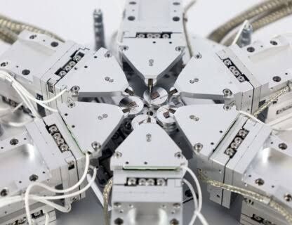
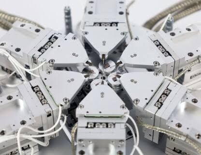
A nano probing system typically combines mechanical positioning, fine probe tips, electrical measurement instruments, and a platform for holding the sample. Depending on the application, the system may also incorporate imaging equipment so that users can locate a specific feature before placing a probe.
How Nanoscale Probing Works
Nanoscale probing equipment is designed around controlled movement. A probe tip must be positioned at a selected point on a sample while avoiding unwanted contact with neighboring structures.
The probe can then establish an electrical connection with the selected feature. Measurements may include voltage, current, resistance, capacitance, or other electrical characteristics, depending on the instruments connected to the probing setup.
A semiconductor nanoprober can be used to examine individual structures within a semiconductor device. Researchers may investigate how a device behaves under different electrical conditions or compare measurements between different regions of a sample.
Main Components of a Nanoprober
Although configurations vary, a nanotechnology measurement equipment setup can contain several core elements:
- Probe arms and fine probe tips for making electrical contact.
- Precision positioning mechanisms for controlled movement.
- A sample stage for holding and positioning the material.
- Imaging equipment for locating measurement points.
- Electrical instruments for applying signals and recording responses.
- Software for controlling measurements and organizing results.
These components work together to create a controlled environment for nanoscale electrical measurement.
Importance
Nanoscale measurement is important because the behavior of a material or electronic device can change when its dimensions become very small. Conventional measurements may combine signals from several structures, making it difficult to determine how an individual component behaves.
A nanoelectronic probing system can isolate particular regions or structures for examination. This can help researchers understand electrical properties at a more localized level.
Supporting Semiconductor Research
Semiconductor probing equipment is used in research involving transistors, interconnects, memory structures, sensors, and other electronic components. Researchers can use probes to investigate individual devices or selected regions of a larger sample.
Semiconductor characterization systems may combine electrical measurements with imaging and other analytical techniques. This can provide information about how physical structure and electrical behavior are related.
Studying Materials and Devices
Nano characterization equipment is also relevant to materials research. Researchers may examine thin films, nanowires, nanoparticles, two-dimensional materials, and other small structures.
Nanotechnology testing equipment can help measure electrical characteristics while researchers vary factors such as applied voltage, temperature, or environmental conditions. The resulting data can contribute to studies of conductivity, resistance, switching behavior, and other properties.
Addressing Measurement Challenges
Working at very small scales creates several technical challenges. Probe placement must be precise, electrical contacts must remain stable, and external electrical noise can interfere with measurements.
The physical properties of the sample can also influence the result. Contact resistance, surface contamination, vibration, temperature changes, and the geometry of the structure may all need to be considered when interpreting measurements.
| Nanoprober Element | Primary Function | Typical Measurement Role |
|---|---|---|
| Probe tip | Makes physical contact | Electrical connection |
| Positioning mechanism | Moves the probe | Precise placement |
| Sample stage | Holds the specimen | Stable testing platform |
| Imaging system | Locates structures | Visual guidance |
| Electrical instrument | Applies or measures signals | Electrical characterization |
| Control software | Coordinates equipment | Measurement management |
Recent Updates
From 2024 through 2026, development in nanoscale probing has generally focused on greater automation, improved positioning control, multimodal measurements, and integration with semiconductor research workflows. These developments reflect the continued reduction in device dimensions and the increasing complexity of nanoscale structures.
Greater Automation
Automated nanoprober systems are being developed to reduce repetitive manual positioning and measurement activities. Automation can coordinate probe movement, measurement sequences, and data collection according to predefined procedures.
Automation does not eliminate the need for measurement planning. Sample preparation, probe selection, electrical settings, and interpretation of results remain important parts of the overall process.
Integration With Imaging and Characterization
Advanced nanoprober systems increasingly combine probing with imaging and other characterization methods. A user may first locate a structure through microscopy and then position a probe for electrical testing.
This integrated approach can connect physical observations with electrical measurements. It is particularly relevant when researchers need to examine a specific nanoscale feature rather than an entire sample.
Semiconductor Device Characterization
Semiconductor research continues to require high precision nanoscale probing as device structures become more complex. Advanced semiconductor probing systems can be configured for different device geometries and measurement procedures.
Nanoscale electrical measurement systems may also be integrated with data acquisition and analysis software. This can make it easier to compare measurements collected across multiple locations or experimental conditions.
Increasing Role of Data Processing
Digital data processing is another area of development. Software can organize measurement sequences, record instrument settings, and assist with visualization of collected data.
Some research environments are also exploring automated analysis methods. These methods can help identify patterns within large measurement datasets, although the interpretation still depends on experimental context and measurement quality.
Tools and Resources
Several tools and resources are useful when learning about or working with nanoprober technology. Their suitability depends on the sample, measurement objective, and laboratory configuration.
Measurement Instruments
A precision nanoprober may be connected to instruments such as source-measure units, digital multimeters, semiconductor parameter analyzers, or impedance measurement equipment. The selected instrument determines which electrical properties can be examined.
Researchers may also use low-noise measurement equipment when signals are particularly small. Proper grounding, shielding, and cable arrangement can help reduce unwanted electrical interference.
Imaging and Positioning Resources
Microscopes and other imaging systems can assist with locating small structures. Optical microscopy may be appropriate for some samples, while electron or scanning probe microscopy can provide additional spatial information for structures beyond conventional optical resolution.
High precision nanoscale probing often depends on combining accurate positioning with suitable imaging. The exact arrangement varies according to the sample and measurement scale.
Reference and Planning Resources
Useful resources include:
- Semiconductor device datasheets and technical documentation.
- Laboratory measurement procedures and calibration records.
- Probe and instrument manuals.
- Semiconductor characterization guides.
- Measurement uncertainty references.
- Research papers on nanoscale electrical characterization.
- Templates for recording probe position, measurement conditions, and results.
Precision nano characterization equipment should be used according to the relevant instrument documentation and laboratory procedures. Measurement results are easier to interpret when experimental conditions are recorded consistently.
FAQs
What is a nanoprober used for?
A nanoprober is used to make controlled electrical contact with very small structures and measure their electrical behavior. Common applications include semiconductor research, nanoelectronics, materials studies, and device characterization.
How do nanoprober systems perform nanoscale electrical measurements?
Nanoprober systems use precisely positioned probe tips to contact selected regions of a sample. Electrical instruments can then apply signals or measure responses such as current, voltage, resistance, or capacitance.
What is a semiconductor nanoprober?
A semiconductor nanoprober is configured for electrical testing and characterization of small semiconductor structures. It can be used to investigate individual devices or selected regions of semiconductor samples.
What is a nano probing system?
A nano probing system combines precision probe positioning with electrical measurement and, in many cases, imaging. It is designed to examine structures that require localized physical and electrical access.
Are automated nanoprober systems fully independent of researchers?
No. Automation can control repeated positioning and measurement sequences, but researchers generally remain responsible for experimental setup, sample preparation, measurement parameters, data validation, and interpretation.
Conclusion
Nanoprobers provide a controlled way to investigate electrical properties at very small physical scales. Nanoprober systems combine precise positioning, probe tips, measurement instruments, sample stages, and supporting software to examine selected structures. Current development is increasingly associated with automation, imaging integration, semiconductor characterization, and digital data handling. These capabilities support research into small electronic devices and materials where localized electrical measurements are needed.